
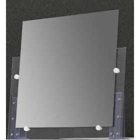
KAKUGATA | Square Silicone Substrate for Advanced Packaging
Addressing the challenges of warping and fine wiring in the PLP process, as well as the thermal issues of the package, by leveraging the properties of silicon.
"Large panelization and miniaturization. Have you given up on achieving both?" Mitsubishi Material's "KAKUGATA" is a square silicon substrate that supports sizes up to 600×600mm. Leveraging the low thermal expansion, high rigidity, and high thermal conductivity derived from silicon, as well as the high flatness and low TTV close to that of wafers, it contributes to improving process challenges associated with the scaling up and miniaturization of FO-PLP and 2.xD packages. Furthermore, by accommodating large panel sizes up to 600×600mm, it also contributes to the enlargement of package sizes and increased productivity. We propose its use for advanced package organic interposer forming carrier substrates, large core substrates, and silicon interposer applications. For more details, please check the Mitsubishi Material official website and consult us through the inquiry form.
